Dual Junction Isolator Technical Analysis: Design and Application Evolution of Broadband High-Isolation RF Devices
Dual Junction Isolator is a non-reciprocal RF device based on multi-port design. It combines dual magnetic circuit structure with broadband matching technology to achieve efficient isolation and low-loss transmission of high-frequency signals. Its core advantages are broadband coverage, high isolation and high power capacity, which are suitable for communication base stations, satellite links, radar systems and other scenarios. This article systematically analyzes the technical principles, structural design, performance parameters, application scenarios and future trends.
1. Technical principles and core features
1. Dual magnetic circuit design and Faraday rotation effect
Dual Junction Isolator uses two independent ferrite magnetic circuits (dual junction structure) to regulate the transmission paths of forward and reverse signals respectively. Based on the Faraday rotation effect, the forward signal passes with low loss (insertion loss <0.5dB), while the reverse signal is absorbed or reflected due to the change in polarization direction, and the isolation can reach 50~60dB (some models such as UIYCDI7038A). Its design supports wide frequency band (such as 10MHz~27.5GHz) operation by optimizing magnetic field uniformity and reducing eddy current loss.
2. Broadband impedance matching
- Hybrid design of coaxial and microstrip lines: Combining the low reflection characteristics of the coaxial interface (N/SMA) with the compact layout of the microstrip line, it ensures 50Ω impedance matching and a standing wave ratio (VSWR) of <1.2.
- Multi-layer substrate integration: Using LTCC (low temperature co-fired ceramic) technology, the ferrite layer is integrated with the transmission line to reduce parasitic parameters (parasitic inductance <0.5nH) and support multi-band coverage (such as UIYCDI6432A covers 700~3500MHz).
3. High power and heat dissipation optimization
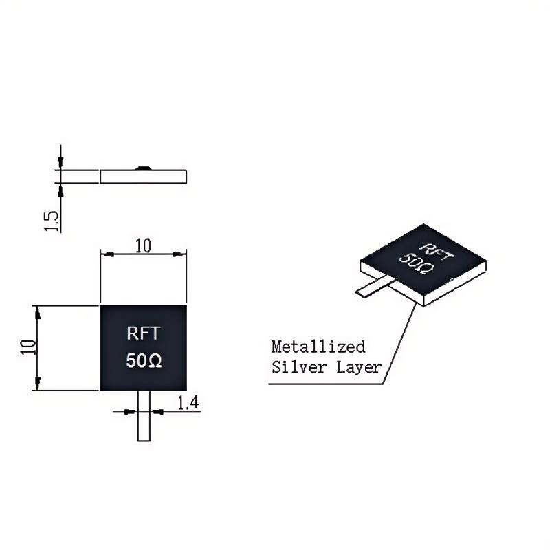
- Power handling capability: Aluminum nitride (AlN) substrate and copper tungsten alloy heat sink combination, continuous wave power up to 300W (such as 7038A), pulse power tolerance 1kW@1μs.
- Thermal management design: Metallized through-holes (Via) conduct heat to the ground layer to ensure stability in high temperature environments (-55℃~+85℃).
2. Structural design and performance parameters
1. Structural classification
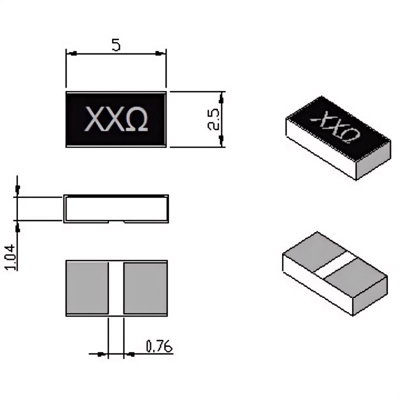
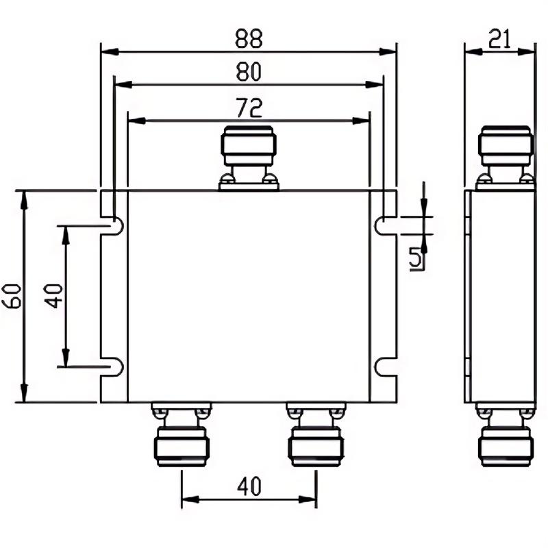
- Coaxial Type: Suitable for high-power scenarios, using metal cavity packaging (such as 16080A size 160×80×28mm), supporting N/SMA interface, power capacity up to 50W@6GHz.
- Drop-in Type: Compact design (such as 5025A size 50.8×25.4×8.6mm), surface mount (TAB interface) adapted to high-density PCB layout, power capacity 200W@2GHz.
3. Typical application scenarios
1. 5G and millimeter wave communication
- Massive MIMO base station: In the Sub-6GHz (n77/n79) and millimeter wave (n258/n260) frequency bands, the isolator protects the power amplifier (PA) from antenna reflection interference and reduces the failure rate of the base station.
- Satellite communication terminal: Ka-band (26.5~40GHz) double-junction isolator suppresses multipath reflection of satellite-to-ground links and is suitable for low-orbit satellite systems such as SpaceX Starlink.
2. Radar and electronic countermeasures
- Phased array radar T/R module: Isolate the transmit and receive channels in the X-band (8~12GHz) to prevent high-power pulses from damaging the low-noise amplifier (LNA).
- Electronic warfare system: Support multi-channel synchronous signal injection to avoid self-oscillation and improve interference efficiency.
3. Test instruments and industrial equipment
- Vector network analyzer (VNA): As a calibration load, it absorbs transient reflection energy (such as 10kV pulse) to ensure measurement accuracy.
- Industrial RF power supply: stabilize the output of the plasma generator and suppress the frequency drift caused by sudden load changes.
IV. Technical challenges and future trends
1. Current technical bottlenecks
- Millimeter wave loss: >30GHz band ferrite eddy current loss increases, and low-dimensional magnetic materials (such as hexagonal ferrite doped with rare earth elements) need to be developed.
- Heat dissipation and power density: 5G millimeter wave band power density >10W/mm², need to be combined with microchannel liquid cooling or diamond substrate technology.
2. Innovation direction
- Intelligent tuning technology: integrated MEMS or liquid crystal materials to achieve dynamic frequency band switching (±15%), adapting to software defined radio (SDR) requirements.
- Photonic-RF hybrid isolation: heterogeneous integration of silicon photonic chips and ferrites, supporting optical-RF co-processing, and reducing transmission losses.
- Green manufacturing: using recyclable magnetic materials and lead-free processes, carbon emissions are reduced by 50%, in line with EU RoHS 3.0 standards.
V. Summary
Dual Junction Isolator has become a core component of high-frequency systems due to its wideband coverage, high isolation and modular design. In the future, with the breakthrough of new materials and intelligent tuning technology, it will evolve towards THz frequency band, self-powered and multi-functional integration, providing key support for 6G inter-sensory integrated network and full coverage of air, land, sea and space.
Publisher: RF Solution http://solutionrf.com/ http://solutionrf.com/logo.png 236 48 ...Please wait.